


The Importance of China UnionPay’s Certification and Letter of Approval
Welcome to our one-off post where we clarify what is meant by Certification and Letter of Approval (LOA) in relation to the recent announcement from FEITIAN (https://ftsafe.com/article/755.html). In this post, David Orme, Senior Vice President for Sales & Marketing at IDEX Biometrics discusses what is meant by Certification and LOA and which IDEX technologies are covered by the Feitian LOA from China Union Pay (CUP).
All payment cards, irrespective of payment network, have many, many boxes to tick before they can enter the marketplace. Each payment network (e.g. CUP, Mastercard, VISA etc.) has its own set of Card Reference Specifications to which card manufacturers must adhere.
These specifications differ from payment network to payment network, but overall cover a series of physical, communication, application, security and performance requirements and tests that are essential to have been met and passed before the payment cards can be offered to market. On completion of the certification process , the relevant laboratory (in this case BCTC) issues a certification report to be analyzed by the payment network, in this case CUP, who then issues the Letter of Approval (LOA). The LOA gives the card manufacturer, in this case, FEITIAN, the go ahead to sell the payment card to card issuers.
It is important to note that without both the Certification and the LOA the card manufacturer cannot go to market with their payment card. This is a multi-step process.
In 2019, CUP issued a new standard specification, “China UnionPay’s Fingerprint Identification Card Technical Guidelines “, which focuses on the regulation of fingerprint technology for identification and security services.
On the 15th April 2020, we were delighted to see our partner, FEITIAN, share the news that their Fingerprint Payment Card had met the requirements of CUP’s Fingerprint Identification Card Technical Guidelines, (their Card Reference Specifications) and therefore officially obtained the CUP LOA, thus becoming the first fingerprint payment card product in the world to obtain this LOA.
As the first fingerprint card product that meets the CUP standard requirements and has passed the CUP product certification, the FEITIAN Fingerprint Payment Card introduces a variety of cutting-edge technologies.
Only with CUP Certification and LOA is Feitian able to kick off taking the product to the card issuers.
FEITIAN LOA FROM CUP
In their release FEITIAN included a scanned copy of the actual LOA received from CUP.
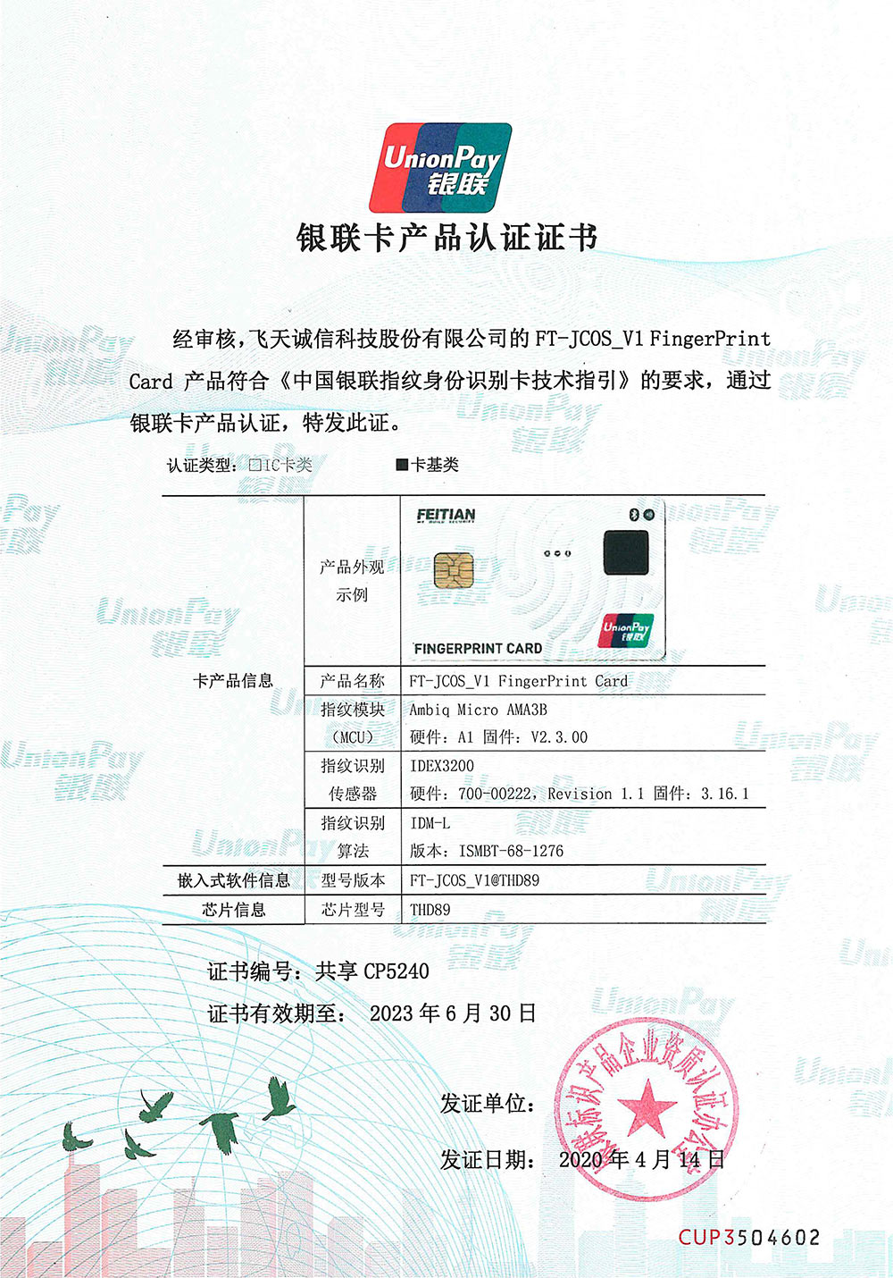
In the image you can see reference to two technologies from IDEX Biometrics. IDEX3200 which is our fingerprint sensor (IDEX Product Name – IDX3200) and IDM-L which is our bespoke matcher.
IDX3200 Fingerprint Sensor
IDX3200 is a durable fingerprint sensor that can be used in dual interface, contactless only and contact only smart cards for payments. IDEX is one of only two suppliers to offer off-chip capacitive fingerprint sensors and the only supplier using this technology with the preferred ridge matching biometric algorithm. IDEX’s off-chip capacitive sensors separate the fingerprint sensing elements from the chip that acquires the image and processes the biometric data. This ingenious design ensures excellent security, significantly higher image fidelity, superb noise immunity and market-leading usability under real-world conditions.
IDM-L Matcher
The embedded matcher is at the heart of the biometric system. It is the biometric verification algorithm that makes the difference between a biometric card that works well and a biometric card that is hard to use.
Key points to note:
- The security requirements imposed by payment schemes mandate that biometric templates are stored securely in the non-volatile memory (NVM) of the Secure Element (SE).
- The matching algorithm must be executed on the SE so that an attacker cannot manipulate any intermediate calculations or matching results that would spoof an incorrect payment authorization
- The available computing power is typically limited to around 100 MHz and the processor cores in use are of Cortex-M class
- SE’s typically have 12-16 Kbyte Static Random-Access Memory (SRAM) and 256-800 Kbyte NVM
- MCU’s typically have 64-128 Kbyte SRAM and 256-512 Kbyte NVM
- Capacitive fingerprint sensors are typically less than 10mm for IDEX off-chip sensing, significantly smaller for silicon sensors.
IDEX Biometrics is very proud that our technologies are key components of FEITIAN’s approved Fingerprint Payment Card.